
| ||
FPGA-Based DPLL Approach
Delivers Wide-Lock Range
Kurt Aronow and Bela Geczy, Mountain
Engineering II, Inc.
Jan 11, 2005 (6:00 AM)
www.MountainEngineering.com
While analog phase-lock loops (PLLs) still have a home in communication
equipment, there is a clear shift in the sector toward implementing digital PLLs
(DPLLs) in comm ASIC designs. For example, in some communication systems,
designers need to implement a synchronous serial port without a separate line to
an external clock. To make this happen, designers need to implement a DPLL that
delivers wide input jitter and wide frequency ranges.
Embedding a DPLL in a comm ASIC is a complex venture. DPLLs require a
significant amount of registers in an ASIC design, making them tough to
implement.
Recently, we had to design an all-digital phase lock loop (DPLL) that could
accommodate a wide input jitter (+/- 180 degrees) range as well as a wide
frequency range (+/-14 percent). The DPLL had to work under conditions when an
input pulse only appeared every four clock periods. The design was part of an
effort to replace an obsolete read channel integrated circuit in a legacy,
18-track linear tape drive. Since the circuit had to be duplicated 18 times, it
needed to occupy as little space as possible in a Xilinx Spartan-IIe FPGA.
However, while this design was developed for a tape-drive application, it could
equally be applied to a communication system requiring a synchronous serial
port.
Although many people have developed phase-lock loops (PLLs) for similar
purposes, they have tended to be buried in proprietary ASICs. So we didn't find
a design similar to what we needed in the literature. Therefore, this article
presents a simple, second-order digital circuit implemented on a field
programmable gate array (FPGA).
DPLL Implementation To achieve the low code and flip-loop counts, we employed several design
tricks. The first trick is to add a small delay into the design so that one can
predict if an input pulse is actually present. So the phase-detector (an edge
detector) only creates an up or down output when there is really an input pulse.
The half-cell delay provides a delay that is approximately half of a DPLL output
clock cycle. If no input pulse appears during that half-cell delay, the edge
detector is not enabled.
Figure 1 below shows a Verilog model for
the proposed DPLL implementation. This Verilog module required only 200 lines of
well-commented code and used 59 synchronous flip-flops.
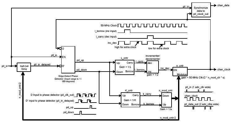
The second trick is to set up a counter (n_mod_cntr) that rolls over at the approximate number of 50 MHz clock cycles so that the DPLL's output frequency approximately matches its input frequency. This modulus counter responds to errors from the phase detector after they are attenuated with the k_cntr. The k_cntr is an up/down counter (with a modulus of K) that provides carry and borrow outputs. Without the k_cntr's attenuation, the output frequency would be unstable.
The third trick is to have a separate, parallel path to adjust for phase differences. The L_cntr is a similar up-down counter to the k_cntr. If the l_cntr asserts the l_carry output, the incrementer/decrementer block removes digital one pulses from a 25 MHz pulse stream (inc_dec). Conversely, if the l_cntr asserts the l_borrow output, the incrementer/decrementer block removes digital one pulses from inc_dec.
If inc_dec spends more time at a digital one level, the n_cntr speeds up. If inc_dec spends more time at a digital zero level, the n_cntr slows down. The modulus of the n_cntr is set with the output of the n_mod_cntr (n_mod_cntr/2). The n_cntr is actually enabled only when inc_dec is high. Note that in order to provide approximately a 50-percent output duty cycle, the n_cntr actually divides by n_mod_cntr/2 twice (taking into account the round-off error due to dividing by n_mod_cntr/2 instead of n_mod_cntr).
Approximating Response
Designers can approximate the frequency
response of the proposed circuit in the s-domain since the DPLL's output
frequency of approximately 1.9 MHz is considerably less than the 50 MHz clock
frequency. The open loop gain of the circuit is:
where: Gain = PD_Gain x Clk / (L x N)
a = L/K
PD_Gain = 1
Our circuit parameters were: Clk = 50 MHz
N = 26 +/- 14% = Clk /
(fc +/-14%)
fc = 1.944 MHz = nominal center
frequency
L = 2
K = 15
These values set the open loop zero at 0.02 Hz, and the 0-dB crossover point at 57 kHz. The time required to adjust for a 14-percent speed variation takes approximately 7 μs. Note that with the zero at such a low frequency, this is essentially a first-order loop. However, without the zero provided by the phase adjust, the circuit would tend to have a large dither.
Wrap Up
DPLLs have become ubiquitous in many ASICs. However, many
registers (and significant design time) are often required to design these
circuits. The design presented here can be implemented in the smallest FPGA for
almost any synchronous serial application. (The design would also fit in many
CPLDs.) The main requirements are a system clock about 50X faster than the
recovered DPLL and regular (although not continuous) bit transmissions.
About the Authors
Bela Geczy is an Senior Analog Engineer at Mountain Engineering II, Inc. He can be reached at bela@mountainengineering.com.
Kurt Aronow is an engineering consultant for Mountain Engineering II, Inc. He can be reached at kurta@mountainengineering.com.
Copyright © 2003 CMP Media, LLC | Privacy Statement